ROSANNAPAPINI.IT
≡
Accessories
Circuitoimpreso
Kits Educativos
Amplifier
Mosfet
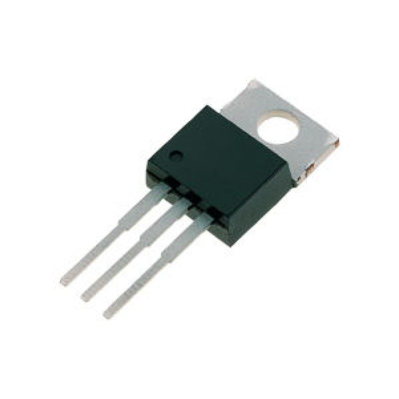
IRF640 Transistor MOSFET in Pakistan
IRF640 Transistor MOSFET in Pakistan
$85.5
$147.92
IRF640 Transistor MOSFET in Pakistan FEATURES SYMBOL QUICK REFERENCE DATA • ’Trench’ technology • Low on-state resistance VDSS = 200 V • Fast switching • Low thermal resistance ID = 16 A RDS(ON) ≤ 180 mΩ GENERAL DESCRIPTION N-channel, enhancement mode field-effect power transistor using Trench technology, intended for use in off-line switched mode power supplies, T.V. and computer monitor power supplies, d.c. to d.c. converters, motor control circuits and general purpose switching applications. The IRF640 is supplied in the SOT78 (TO220AB) conventional leaded package. The IRF640S is supplied in the SOT404 (D2 PAK) surface mounting package. PINNING SOT78 (TO220AB) SOT404 (D2 PAK) AVALANCHE ENERGY LIMITING VALUES Limiting values in accordance with the Absolute Maximum System (IEC 134) SYMBOL PARAMETER CONDITIONS MIN. MAX. UNIT EAS Non-repetitive avalanche Unclamped inductive load, IAS = 6.2 A; – 580 mJ energy tp = 720 µs; Tj prior to avalanche = 25˚C; VDD ≤ 25 V; RGS = 50 Ω; VGS = 10 V; refer to fig;14 IAS Peak non-repetitive – 16 A avalanche current THERMAL RESISTANCES SYMBOL PARAMETER CONDITIONS MIN. TYP. MAX. UNIT Rth j-mb Thermal resistance junction – – 1.1 K/W to mounting base Rth j-a Thermal resistance junction SOT78 package, in free air – 60 – K/W to ambient SOT404 package, pcb mounted, minimum – 50 – K/W footprint ELECTRICAL CHARACTERISTICS Tj = 25˚C unless otherwise specified SYMBOL PARAMETER CONDITIONS MIN. TYP. MAX. UNIT V(BR)DSS Drain-source breakdown VGS = 0 V; ID = 0.25 mA; 200 – – V voltage Tj = -55˚C 178 – – V VGS(TO) Gate threshold voltage VDS = VGS; ID = 1 mA 2 3 4 V Tj = 175˚C 1 – – V Tj = -55˚C – 6 V RDS(ON) Drain-source on-state VGS = 10 V; ID = 8 A – 130 180 mΩ resistance Tj = 175˚C – – 522 mΩ IGSS Gate source leakage current VGS = ± 20 V; VDS = 0 V – 10 100 nA IDSS Zero gate voltage drain VDS = 200 V; VGS = 0 V; – 0.05 10 µA current VDS = 160 V; VGS = 0 V; Tj = 175˚C – – 250 µA Qg(tot) Total gate charge ID = 18 A; VDD = 160 V; VGS = 10 V – – 63 nC Qgs Gate-source charge – – 12 nC Qgd Gate-drain (Miller) charge – – 35 nC td on Turn-on delay time VDD = 100 V; RD = 5.6 Ω; – 12 – ns tr Turn-on rise time VGS = 10 V; RG = 5.6 Ω – 45 – ns td off Turn-off delay time Resistive load – 54 – ns tf Turn-off fall time – 38 – ns Ld Internal drain inductance Measured tab to centre of die – 3.5 – nH Ld Internal drain inductance Measured from drain lead to centre of die – 4.5 – nH (SOT78 package only) Ls Internal source inductance Measured from source lead to source – 7.5 – nH bond pad Ciss Input capacitance VGS = 0 V; VDS = 25 V; f = 1 MHz – 1850 – pF Coss Output capacitance – 170 – pF Crss Feedback capacitance – 91 – pF August 1999 2 Rev 1.100 Philips Semiconductors Product specification N-channel TrenchMOS transistor IRF640, IRF640S REVERSE DIODE LIMITING VALUES AND CHARACTERISTICS Tj = 25˚C unless otherwise specified SYMBOL PARAMETER CONDITIONS MIN. TYP. MAX. UNIT IS Continuous source current – – 16 A (body diode) ISM Pulsed source current (body – – 64 A diode) VSD Diode forward voltage IF = 18 A; VGS = 0 V – 1.0 1.5 V trr Reverse recovery time IF = 18 A; -dIF/dt = 100 A/µs; – 130 – ns Qrr Reverse recovery charge VGS = 0 V; VR = 25 V – 0.8 – µC
Mosfet
Mosfet
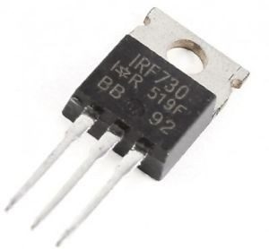
IRF730 Power MOSFET 400v 3.5A in Pakistan
$40.5
$58.73
C1815 Transistor NPN Transistor Price In Pakistan
$33.84
$48.39
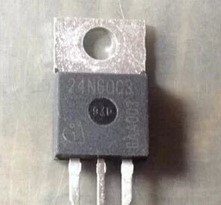
24N60 SPP24N60C3 24N60C3 TO-220 in Pakistan
$37.02
$71.45
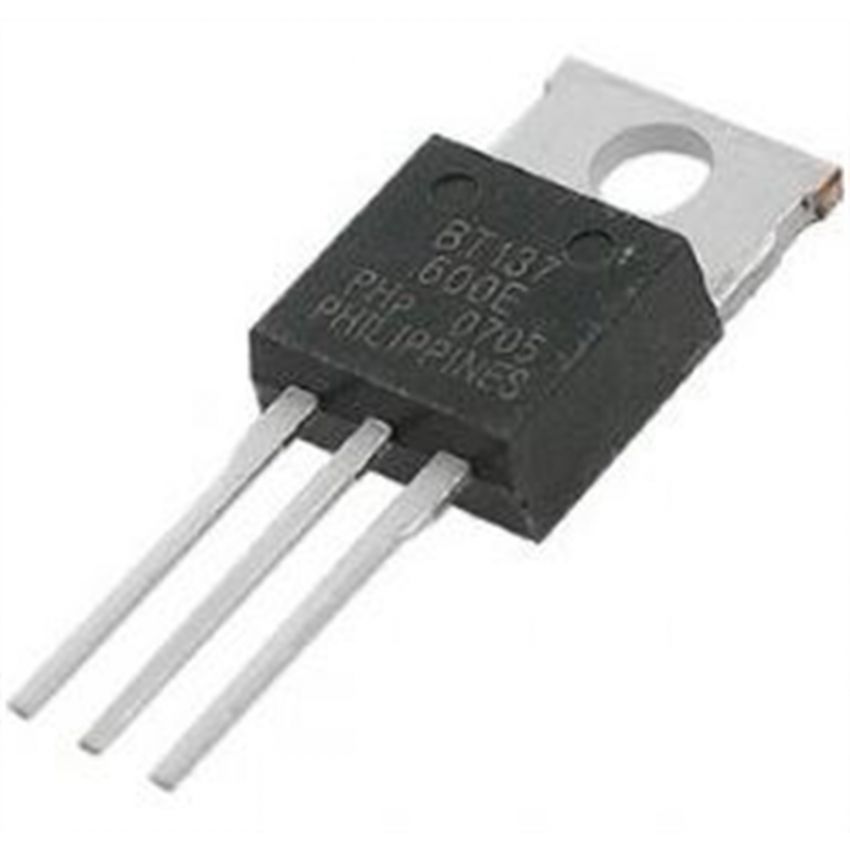
BTA137 TRIAC in Pakistan
$45
$66.15
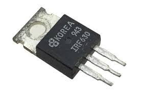
IRF630 MOSFET Transistor Set – 3PCS N-Channel 200V 9A
$76.5
$135.41
Audio Amplifier D313 NPN Transistor in Pakistan
$22.5
$40.95
CDIL C106D in Pakistan
$54
$78.3
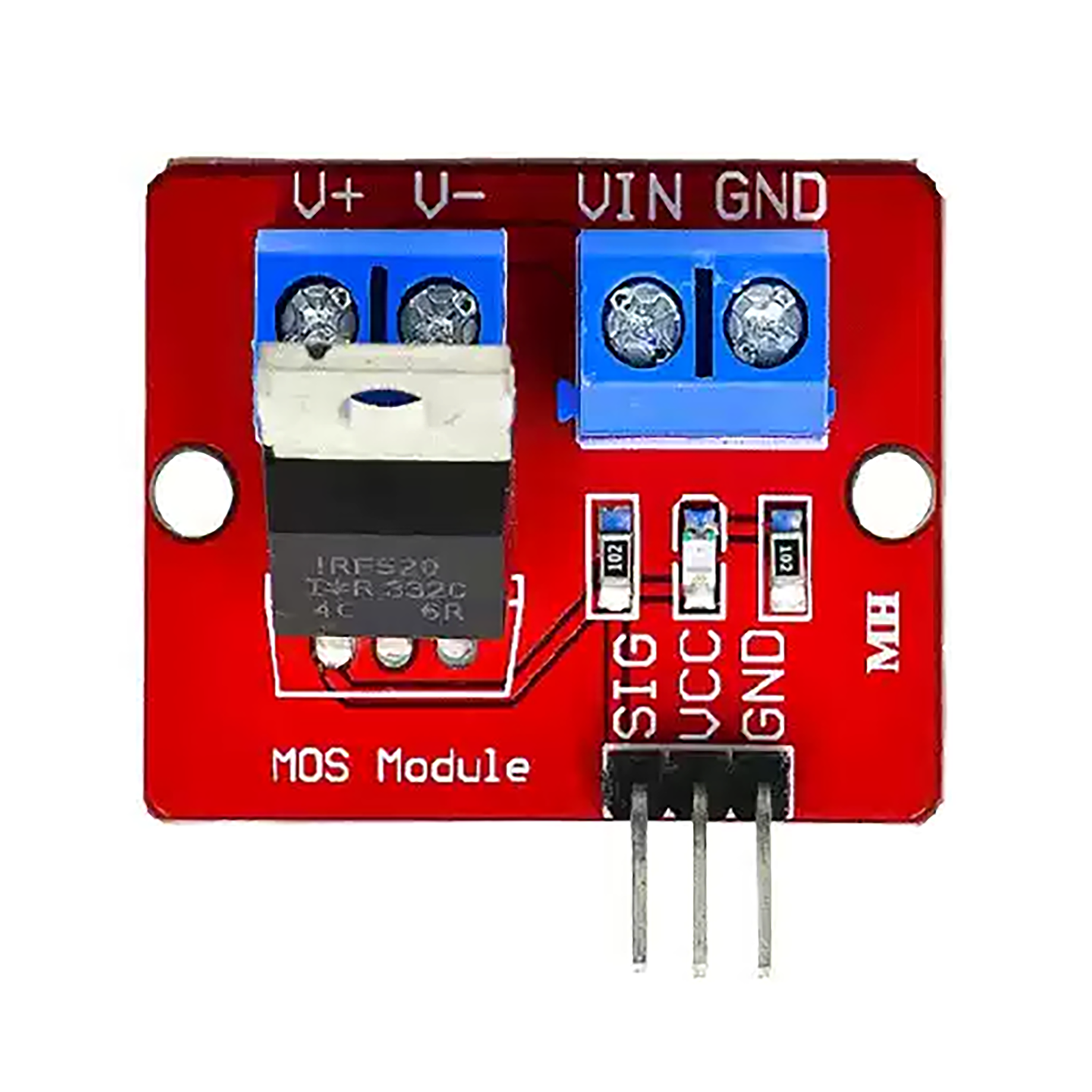
IRF520 MOSFET PWM Adjustment Module
$26.01
$47.34
BTA16 600b 16Amp Triac
$45
$77.4
Aluminum Heatsink for IC,MOSFET,Trasistor, SCR etc
$40.5
$69.66
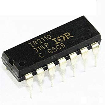
IR2110 IR 2110 IC High and Low Side MOSFET Driver
$62.56
$97.59
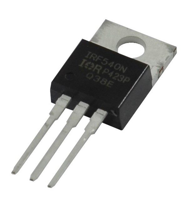
IRF540 N-Channel Power MOSFET
$81
$155.52
IRF640 Transistor MOSFET in Pakistan
$85.5
$147.92